Optical characterization of deep-ultraviolet AlGaN LEDs
Light in the deep ultraviolet (DUV) wavelength regime, with wavelengths below 300 nm, has the ability to inactivate pathogenic microbes. For this reason, DUV light is useful in fields such as medicine, water purification, sterilization, and disinfection. Currently, 785 million people on earth live without access to even basic drinking water. Therefore, realization of a solid-state DUV light source that can be operated with low voltage and high efficiency at a low cost and its wide implementation in society are important. We are working on the characterization of the optical properties of DUV light-emitting diodes (LEDs) involving aluminum gallium nitride (AlGaN), a material with the potential to meet these demands.

References:
K. Kojima, Y. Nagasawa, A. Hirano, M. Ippommatsu, Y. Honda, H. Amano, I. Akasaki, and S. F. Chichibu,
"Carrier localization structure combined with current micropaths in AlGaN quantum wells grown on an AlN template with macrosteps",
Appl. Phys. Lett. 114, 011102 (2019).
DOI: 10.1063/1.5063735
小島一信, 長澤陽祐, 平野光, 一本松正道, 杉江隆一, 本田善央, 天野浩, 赤﨑勇, 秩父重英,
"マクロステップを持つc面AlN/サファイアテンプレート上に成長させたAlGaN量子井戸の物性評価",
日本結晶成長学会誌 (Journal of the Japanese Association for Crystal Growth) 47, 1-8 (2020).
DOI: 10.19009/jjacg.47-3-04
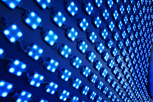
High-speed solar-blind optical wireless communication system with DUV LEDs
Optical wireless communication technology based on inexpensive light sources such as LEDs is gaining recognition as a key technology for the 6th generation mobile communication system (6G). DUV light is almost completely absent from solar radiation at the earth's surface, which makes the DUV wavelength band insensitive to sunlight, known as the "solar blind" band, and is expected to allow optical wireless communications in low-noise environments even outdoors during the daytime. We are working on the realization of a Gbps class high-speed optical wireless communication system using DUV LEDs and on the elucidation of the high-speed modulation mechanism of DUV LEDs.
References:
K. Kojima, Y. Yoshida, M. Shiraiwa, Y. Awaji, A. Kanno, N. Yamamoto, and S. F. Chichibu,
"1.6-Gbps LED-based ultraviolet communication at 280 nm in direct sunlight",
2018 European Conference on Optical Communication (ECOC) (2018).
DOI: 10.1109/ECOC.2018.8535544
Y. Yoshida, K. Kojima, M. Shiraiwa, Y. Awaji, A. Kanno, N. Yamamoto, S. F. Chichibu, A. Hirano, and M. Ippommatsu,
"An outdoor evaluation of 1-Gbps optical wireless communication using AlGaN-based LED in 280-nm band",
2019 Conference on Lasers and Electro-Optics (CLEO) (2019).
DOI: 10.1364/CLEO_SI.2019.SM2G.1
K. Kojima, Y. Yoshida, M. Shiraiwa, Y. Awaji, A. Kanno, N. Yamamoto, A. Hirano, Y. Nagasawa, M. Ippommatsu, and S. F. Chichibu,
"Self-organized micro-light-emitting diode structure for high-speed solar-blind optical wireless communications",
Appl. Phys. Lett. 117, 031103 (2020).
DOI: 10.1063/5.0013112
小島一信, 秩父重英, 吉田悠来, 白岩雅輝, 淡路祥成, 菅野敦史, 山本直克, 長澤陽祐, 平野光,
"窒化アルミニウムガリウム深紫外発光ダイオードを用いたギガビット級ソーラーブラインド光無線通信",
月刊OPTRONICS 6月号 (2020). ISSN: 02869659
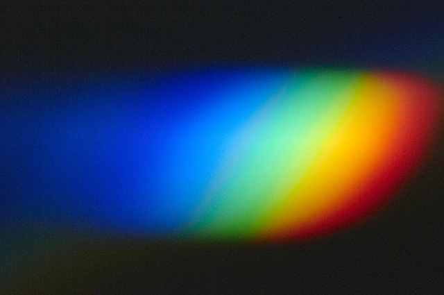
Development and application of omnidirectional photoluminescence (ODPL) spectroscopy
The development of technologies for efficient use of limited energy resources is necessary to realize a sustainable society. For example, electronic devices such as diodes and transistors that can rectify current and convert voltage with high breakdown voltage and low loss are important for applications such as railroads and electric vehicles that transform electricity into strong power for use. In the fields of lighting, communications, and solar power generation, it is essential to increase the efficiency of optical devices such as light-emitting diodes, semiconductor lasers, and solar cells, which convert electrical energy and light energy into each other. Since these semiconductor devices are fabricated on crystal substrates called wafers, it is no exaggeration to say that the performance of the devices depends on the quality of the crystals that constitute the wafers. In particular, gallium nitride (GaN) is attracting attention as a material suitable for manufacturing high-performance electronic and optical devices, and competition to develop high-quality GaN wafers is intensifying in Japan and overseas.
The widespread use of semiconductor devices requires the large-scale mass production of wafers, and in the case of GaN, circular wafers with a diameter of 6 inches (approximately 152 mm) or more are desired. In order to control the quality of such large GaN wafers, an inspection method that can examine the entire wafer surface with high speed and high sensitivity is essential. We have developed an omnidirectional photoluminescence (ODPL) spectroscopy, a high-precision characterization technique for semiconductor crystals that can meet these requirements.
References:
K. Kojima, T. Ohtomo, K. Ikemura, Y. Yamazaki, M. Saito, H. Ikeda, K. Fujito, and S. F. Chichibu,
"Determination of absolute value of quantum efficiency of radiation in high quality GaN single crystals using an integrating sphere",
J. Appl. Phys. 120, 015704 (2016).
DOI: 10.1063/1.4955139
K. Kojima, K. Ikemura, and S. F. Chichibu,
"Quantification of the quantum efficiency of radiation of a freestanding GaN crystal placed outside an integrating sphere",
Appl. Phys. Express 12, 062010 (2019).
DOI: 10.7567/1882-0786/ab2165
K. Kojima, K. Ikemura, and S. F. Chichibu,
"Temperature dependence of internal quantum efficiency of radiation for the near-band-edge emission of GaN crystals quantified by omnidirectional photoluminescence spectroscopy",
Appl. Phys. Express 13, 105504 (2020).
DOI: 10.35848/1882-0786/abb788
ODPL分光法を応用した製品(浜松ホトニクス株式会社)
https://www.hamamatsu.com/jp/ja/product/type/C15993-01/index.html
全方位フォトルミネセンス(ODPL)分光法を用いた半導体結晶の評価
https://doi.org/10.11470/oubutsu.90.12_726
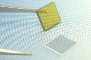
Characterization of perovskite semiconductors toward optical cooling
The mainstream of development in electronic and optical devices based on semiconductors is aimed at energy conservation, i.e., low loss and high efficiency. For example, the power conversion loss of power transistors has been reduced to a few percent, and the efficiency of blue LEDs was reported to exceed 80%. On the other hand, thermoelectric conversion devices, which control thermal energy electrically, have also been studied by using polycrystalline semiconductors and metallic materials, but the current status is still less efficient than the various semiconductor devices mentioned above.
We are working to improve the internal quantum efficiency (IQE) of radiation of metal halide perovskite semiconductors, which are known as crystals for high-efficiency solar cells, to close to 100%. IQE is the probability that excited electron-hole pairs in a crystal generate photons. If the IQE is close to 100%, cooling of the material by the optical cooling phenomenon is expected.

References:
K. Kojima, K. Ikemura, K. Matsumori, Y. Yamada,
Y. Kanemitsu, and S. F. Chichibu, "Internal
quantum efficiency of radiation in a bulk CH3NH3PbBr3 perovskite crystal
quantified by using the omnidirectional photoluminescence spectroscopy'',
APL Materials 7(7), 071116 (2019).
DOI:
10.1063/1.5110652
Y. Kajino, S. Otake, T. Yamada, K. Kojima, T. Nakamura, A. Wakamiya, Y. Kanemitsu, and Y. Yamada,
"Anti-Stokes photoluminescence from CsPbBr3 nanostructures embedded in a Cs4PbBr6 crystal",
Phys. Rev. Materials 6, L043001 (2022).
DOI: 10.1103/PhysRevMaterials.6.L043001
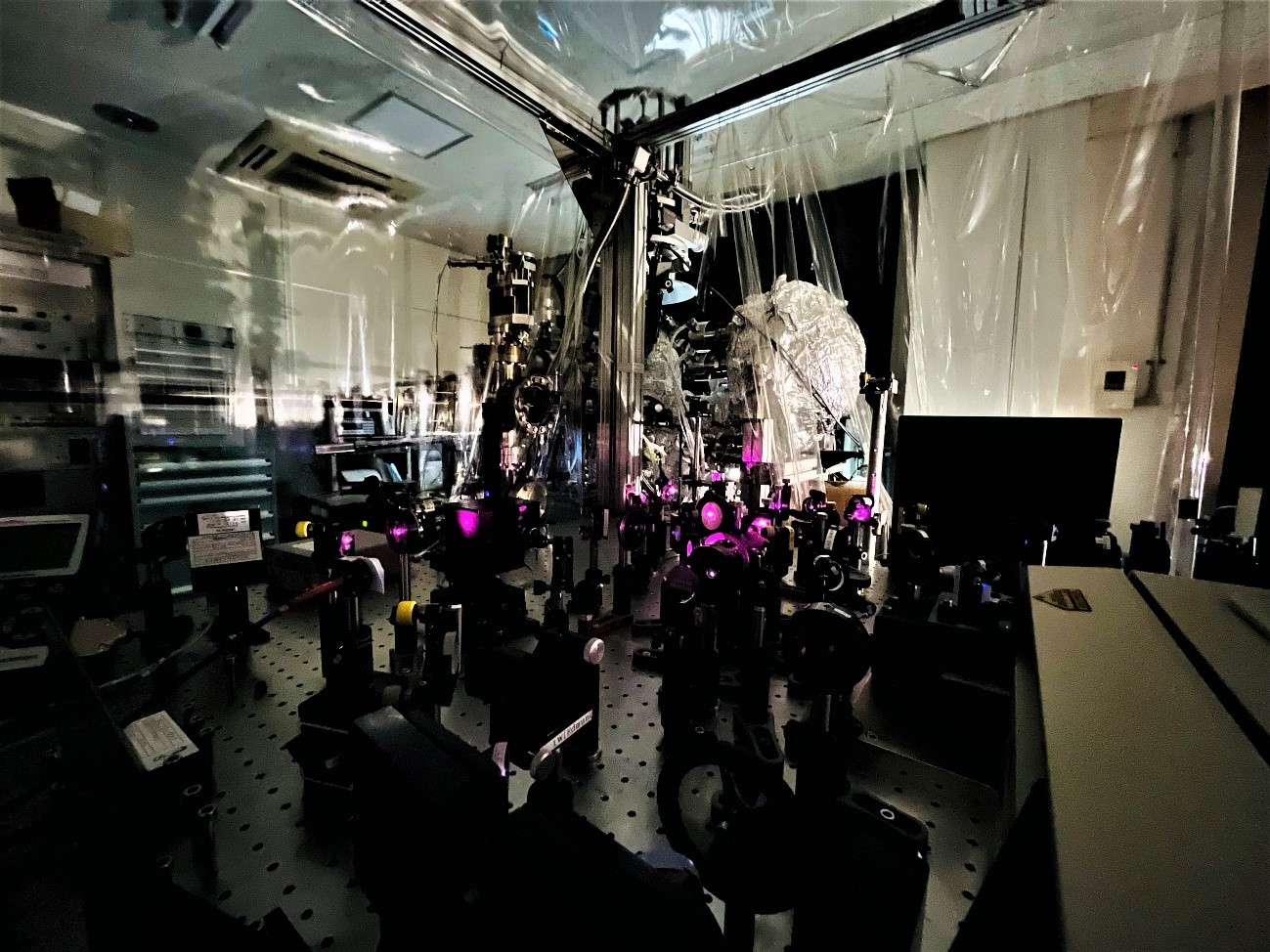
Time-resolved two-photon photoemission spectroscopy for characterization of next-generation semiconductor materials
The recent development of spectroscopic techniques using ultrashort laser pulses has made it possible to elucidate high-speed physical phenomena in materials. In solid state materials, electron interaction or relaxation processes are known to occur on a time scale from a few femtoseconds to hundreds of femtoseconds, and in order to elucidate the dynamic behavior of electrons injected into semiconductor devices until their energy dissipation, high-precision time-resolved characterization on the order of femtoseconds to nanoseconds is required. By combining a femtosecond pulsed laser generator and a photoelectron spectrometer, we have developed a time-resolved two-photon photoemission spectroscopy (TPS) measurement system, and are working on the dynamic characterization of electrons in next-generation semiconductor materials such as gallium nitride (GaN) semiconductors. In particular, we are promoting research on the effects of crystal defects in semiconductors upon device operation from the viewpoints of both device development and physical property characterization.
References:
S. Ichikawa, Y. Fujiwara, and K. Kojima,
"Visualization of Excited-Electron Relaxation in InGaN Quantum Wells using Time-Resolved Two-Photon Photoemission Spectroscopy",
International Workshop on Nitride Semiconductors 2022, AT 003, Berlin, Germany (Oct. 2022).
市川 修平, 毎田 修, 小島 一信,
"二光子光電子分光によるGaAs(110)における表面再結合寿命の評価",
第42回ナノテスティングシンポジウム NANOTS 2022, (15), 千里ライフサイエンスセンター 豊中市 (Nov. 2022).
市川 修平, 松田 祥伸, 道上 平士郎, 毎田 修, 船戸 充, 川上 養一, 小島 一信,
"時間分解二光子光電子分光法によるInGaN (0001)の表面キャリア寿命測定",
第70回応用物理学会春季学術講演会, 16a-B401-5, 上智大学四谷キャンパス (March 2023).
S. Ichikawa, Y. Matsuda, H. Dojo, M. Funato, Y. Kawakami, and K. Kojima,
"Surface carrier lifetime of (0001) InGaN assessed by time-resolved photoemission spectroscopy",
The 14th International Conference on Nitride Semiconductors (ICNS-14), CH1-2, Fukuoka, Japan (Nov. 2023).
Development of evaluation method for diamond semiconductor crystal
Diamond electronic devices are expected to be the next generation of power devices and high-frequency devices, and further improvement of the quality of homoepitaxial CVD thin films is essential for their realization. In the past, cathodoluminescence and photoluminescence have been used to characterize the light emitting process in diamond to clarify the key factors for improving the quality. However, as the quality of CVD diamond films has been improved, it has become important to characterize and control nonradiative defects that cannot be detected by conventional methods based on the luminescence process. Therefore, we are developing an appropriate characterization system for nonradiative defects in wide bandgap semiconductors and searching for the key factors to improve the quality of CVD diamond films.
References:
望月 梧生, 毎田 修, 金 聖祐, 加藤 学, 小山 浩司, 本田 達也, 市川 修平, 小島 一信,
"Ir/sapphire基板上ヘテロエピタキシャル成長(001)面ダイヤモンド膜の断面SEM像に見られる縞状コントラストの分析",
第84回応用物理学会秋季学術講演会, 21p-C402-4, 熊本城ホール他 (Sep. 2023).